MIR-3306-TC11中文资料
SMD Type Reflective Photo Sensor
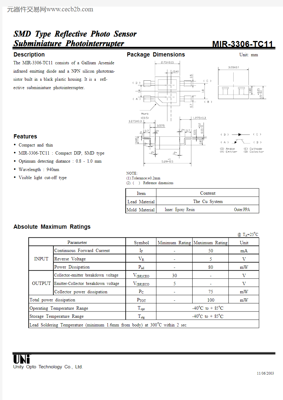
Subminiature Photointerrupter MIR-3306-TC11 Description Package Dimensions Unit: mm
Features
Compact and thin
Wavelength : 940nm
Visible light cut-off type
Item
Lead Material
Mold Material
Absolute Maximum Ratings
@ T A=25o C
Symbol Minimum Rating Maximum Rating Unit
I F-50mA
V R-5V
P ad-80mW Collector-emitter breakdown voltage V(BR)CEO30-V
Emitter-Collector breakdown voltage V(BR)ECO5-V
Collector power dissipation P C-75mW
P TOT-100mW
T opr
T stg
Content
The Cu System Lead Soldering Temperature (minimum 1.6mm from body) at 300o C within 2 sec
Total power dissipation
Operating Temperature Range
Storage Temperature Range
-40o C to + 85o C
-40o C to + 85o C INPUT
OUTPUT
Inner: Epoxy Resin Outer:PPA
Parameter
Reverse Voltage
Power Dissipation
Continuous Forward Current
NOTE:
(1).Tolerance:±0.2mm
(2). ( ) Reference dimensions
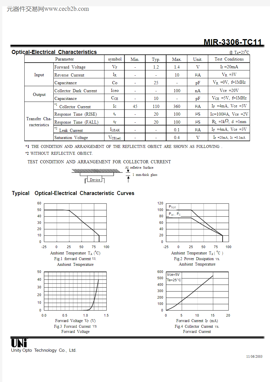
Optical-Electrical Characteristics
@ T A =25o C
Min.
Typ.Max.Unit.Forward Voltage
- 1.2 1.4V Reverse Current --10μA
Capacitance
-25-pF Collector Dark Current --100nA Capacitance
-10-pF *1
Collector Current
45110360μA Response Time (RISE)
-20100μS Response Time (FALL)
-20100μS *2
Leak Current
--0.1μA Saturation Voltage
-
-
0.4
V
*1 THE CONDITION AND ARRANGEMENT OF THE REFLECTIVE OBJECT ARE SHOWN AS FOLLOWING .
*2 WITHOUT REFLECTIVE OBJECT.
TEST CONDITION AND ARRANGEMENT FOR COLLECTOR CURRENT
Typical Optical-Electrical Characteristic Curves
I F =4mA, Vce =3V I F =20mA, Ic =0.1mA
Input
Parameter Transfer Cha-racteristics
V CE(set)
Test Conditions I F =20mA V R =3V V R =0V, f=1MHz R L =1k ?, d =1mm symbol V F I R Iceo Co Vce =20V V CE =5V, f=1MHz I F =4mA, Vce =3V Ic=100μA, Vce =2V Output
C CE
I LEAK t f t r
Ic 1 mm-thick glass
020406080100120-25
0255075
100
Ambient Temperature T
A (o
C)Fig.1 forward Current VS .Ambient Temperature
F o r w a r d C u r r e n t I F (m A )
Ambient Temperature T A ( o
C )Fig.2 Power Dissipation vs.Ambient Temperature
P o w e r D i s s i p a t i o n (m W )
0102030405060-25
25
50
75
100C o l l e c t o r C u r r e n t I c (μA )
01002003004005006000
5101520
F o r w a r d C u r r e n t I F (m A )
Forward Current I F (mA)Fig.4 Collector Current vs.
Forward Current
010*********.0
0.5
1.0
1.5
Forward Voltage V F (V)Fig.3 Forward Current VS
Forward Voltage
Typical Optical-Electrical Characteristic Curves Test Circuit for Response Time
50
100
150
200
250
300
350
024681012
C
o
l
l
e
c
t
o
r
C
u
r
r
e
n
t
I
c
(
μ
A
)
Collector-Emitter Voltage Vce (V)
Fig.5 Collector Current vs. Vce
20
40
60
80
100
120
-250255075100
R
e
l
a
t
i
v
e
C
o
l
l
e
c
t
o
r
C
u
r
r
e
n
t
(
%
)
Ambient Temperature T A (o C)
Fig.6 Relative Collector Current VS.
025*******
C
o
l
l
e
c
t
o
r
D
a
r
k
C
u
r
r
e
n
t
I
C
E
O
Ambient Temperature T A (o C)
Fig.7 Collector Dark Current vs.
Ambient Temperature
R
e
s
p
o
n
s
e
T
i
m
e
(
μ
s
)
Load Resistance R t (K?)
Fig.8 Response Time vs.
Load Resistance
R
e
l
a
t
i
v
e
C
o
l
l
e
c
t
o
r
C
u
r
r
e
n
t
(
%
)
20
40
60
80
100
700800900100011001200
R
e
l
a
t
i
v
e
S
e
n
s
i
t
i
v
i
t
y
(
%
)
Wavelength (nm)
Fig.9 Spectral Sensitivity (Detecting side)
20
40
60
80
100
120
012345678910
Distance (mm)
Fig.10 Relative Collector Current vs. Distance
between MIR-3306 and Card
0.1
1
10
100
0.010.1110
Test Item Description and Test Condition Reference Standard Judgement
Operation Life Evaluates resistance of the device when operated at electrical stress Ta=under room temperature Test Time=1000hrs
(-24hrs,+72hrs)
MIL-STD-750:1026
MIL-STD-883:1005
JIS C 7021:B-1
ACCEPT:
Power Decay <30%
High Temperature
High Humidity
Evaluates moisture resistance of the device
when stored for a long term at high
temperature and high humidityTa=85±5o C
Rh=85±5%RhTest Time=1000hrs
(-24hrs,+72hrs)
MIL-STD-202:103B
JIS C 7021:B-11
ACCEPT:
None is
OPEN/SHORT
High Temperature
Storage
Evaluates device durability for long term
storage in high temperature Ta=105o C
Test Time=1000hrs(-24hrs,+72hrs)
MIL-STD-883:1008
JIS C 7021:B-10
ACCEPT:
None is
OPEN/SHORT Low Temperature
Storage
Evaluates device durability for long term
storage in low temperature Ta=-55o C
Test Time=1000hrs(-24hrs,+72hrs)
JIS C 7021:B-12
ACCEPT:
None is
OPEN/SHORT Temperature Cycling
Evaluates resistance of device at thermal
stresses or expansion and contraction
105o C ~ 25o C ~ -55o C ~ 25o C
30min 5min 30min 5min 20 Cycles
MIL-STD-202:107D
MIL-STD-750:1051
MIL-STD-883:1010
JIS C 7021:A-4
ACCEPT:
None is
OPEN/SHORT Thermal Shock
Evaluates device’s structure and mechanical
resistance when suddenly exposed at severe
changes
105o C ~ -55o C
10min 10min 10 Cycles
MIL-STD-202:107D
MIL-STD-750:1051
MIL-STD-883:1011
ACCEPT:
None is
OPEN/SHORT
Reflow Soldering
Heat Resistance Test
Reflow process : Condition is as follow
page. Less than 2 time.
MIL-STD-202:210A
MIL-STD-750:2031
JIS C 7021:A-1
ACCEPT:
None is
OPEN/SHORT Solderability
Evaluates solderability on leads of device
T.Sol=230o C
Dwell Time=5 sec
MIL-STD-202:208D
MIL-STD-750:2026
MIL-STD-883:2003
JIS C 7021:A-2
ACCEPT:
95% soldering areaon
the lead frame
PresureCooker Test
Phase1:110o C, 85%RH, 1.242kgf/cm2
Phase2:130o C, 85%RH,2.714kgf/cm2
-
ACCEPT:
None is
OPEN/SHORT Drop Test
Distance of Dropping : 1 m
Drop the Device on the Maple Board
3 Times
-
ACCEPT:
None is
OPEN/SHORT
Reliability Test Item
1. Reflow Soldering.
2. Dip Soldering.
RECOMMENDED SOLDERING CONDITION
5 sec. MAX soldering time
- 5 o C /sec. MAX
1.a The above temp. profile shall be at the surface of LED resin.
1.b Number of reflow process should be less than 2 times.If the second reflow process is
performed, intervals between the first and the second process should be as short as possible to prevent moisture absorption from LED resin. Cooling process to normal temp. is required between the first and the second reflow process.
1.c Temp. fluctuation to LED at pre-heat process should be minimized. ( less than 6 o C )
2.a. Preheat temp. for soldering : 120 - 150 o
C, 60 - 120 sec.
2.b. Soldering temp.: Temp. of soldering pot 300 o C Max and soldering time less than 2 sec. 2.c. Number of dip soldering process must be less than 2 times and the process is performed in sequrence. Cooling process to normal temp. will be required between the first and the second soldering process.
Tape Dimensions
Unit:mm
REEL Dimensions
Quantity : 1000pcs
Taping Construction
1. The sproket holes shall be on the left side against the pull-out direction.
2.The space of more than 20 pitches shall be provided on each front of tape mounting.
3.The space of more than 40 mm shall be provided on each rear of tape mounting.
4.The leader of more than 400 mm by the cover tape shall be provided at the pull-out start portion.
Taping Mechanical characteristics and specifications
1. Peeling strength of cover tape :
(1). F=0.2~0.7N(20~70gf)(measure by tension gage)
(2). Tape should not be burst by peeling.
2. Specifications :
(1). When the tape is bent to radius 30 mm, products do not fall down from the tape and tape doesn't
get any gamage.
(2). During the peeling, products do not fix to cover tape.
(3). The product which was enclossed in reverse direction or with back side up should be count as
0pcs/reel. The number of dropped parts should be 0.1% reel.
PACKAGE LABEL
MIR-3306-TC11