TSL3301中文资料
1
Copyright E 2001, TAOS Inc.
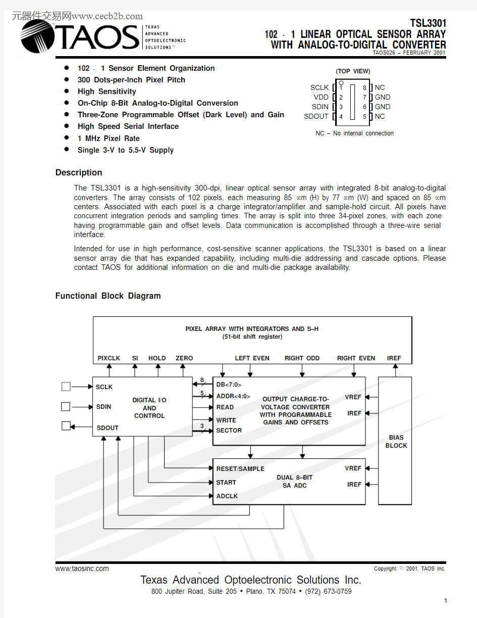
D 102 × 1 Sensor Element Organization D 300 Dots-per-Inch Pixel Pitch D High Sensitivity
D On-Chip 8-Bit Analog-to-Digital Conversion
D Three-Zone Programmable Offset (Dark Level) and Gain D High Speed Serial Interface D 1 MHz Pixel Rate
D
Single 3-V to 5.5-V Supply
Description
The TSL3301 is a high-sensitivity 300-dpi, linear optical sensor array with integrated 8-bit analog-to-digital converters. The array consists of 102 pixels, each measuring 85 μm (H) by 77 μm (W) and spaced on 85 μm centers. Associated with each pixel is a charge integrator/amplifier and sample-hold circuit. All pixels have concurrent integration periods and sampling times. The array is split into three 34-pixel zones, with each zone having programmable gain and offset levels. Data communication is accomplished through a three-wire serial interface.
Intended for use in high performance, cost-sensitive scanner applications, the TSL3301 is based on a linear sensor array die that has expanded capability, including multi-die addressing and cascade options. Please contact TAOS for additional information on die and multi-die package availability.
Functional Block Diagram
SCLK VDD SDIN SDOUT
NC GND GND NC
(TOP VIEW)
NC – No internal connection
TAOS026 – FEBRUARY 2001
2
https://www.docsj.com/doc/6c1426854.html,
t
t
Copyright E 2001, TAOS Inc.
Terminal Functions
Detailed Description
The TSL3301 is a 102 × 1 linear optical array with onboard A/D conversion. It communicates over a serial digital interface and operates over a 3 V to 5.5 V range. The array is divided into three 34-pixel zones (left, center, and right), with each zone having programmable gain and offset (dark signal) correction.
The sensor consists of 102 photodiodes, also called pixels, arranged in a linear array. Light energy impinging on a pixel generates a photocurrent, which is then integrated by the active integration circuitry associated with that pixel. During the integration period, a sampling capacitor connects to the output of the integrator through an analog switch. The amount of charge accumulated at each pixel is directly proportional to the light intensity (E e ) on that pixel and to the integration time (t int ). At maximum programmed gain, one LSB corresponds to approximately 300 electrons.
Integration, sampling, output, and reset of the integrators are performed by the control logic in response to commands input via the SDIN pin. Data is read out on the SDOUT pin. A normal sequence of operation consists of a pixel reset (RESET ), start of integration (STARTInt ), integration period, sampling of integrators (SAMPLEInt ), and pixel output (READPixel ). Reset sets all the integrators to zero. Start of integration releases the integrators from the reset state and defines the beginning of the integration period. Sampling the integrators ends the integration period and stores the charge accumulated in each pixel in a sample and hold circuit.Reading the pixels causes the sampled value of each pixel to be converted to 8-bit digital format and output on the SDOUT pin. All 102 pixels are output sequentially unless interrupted by an abort (ABORTPixel ) command or reset by a RESET command.
Gain adjustment is controlled by three 5-bit DACs, one for each of the the three zones. Table 1 lists the gain settings and the corresponding pixel values. Offset is affected by the gain setting and may have to be adjusted after gain changes are made.
Offset correction is controlled by three 8-bit sign-magnitude ? DACs and is performed in the analog domain prior to the digital conversion. There is a separate offset DAC for each of the three zones. Codes 0h – 7Fh correspond to positive offset values and codes 80h – FFh correspond to negative offset values.
The offset correction is proportional to the gain setting. At minimal gain, one LSB of the offset DAC corresponds to approximately 1/3 LSB of the device output, and at maximum gain, to about 1 LSB of the device output.Note that the gain and offset registers are in indeterminate states after power up and must be set by the controller as required.
?
Sign-magnitude is a binary representation in which the most significant bit (MSB) is used to represent the sign of the number, with the remaining bits representing the magnitude. An MSB of 1 indicates a negative number.
t
t Copyright E 2001, TAOS Inc.
Table 1. Gain Settings and Results
Serial interface
The serial interface follows a USART format, with start bit, 8 data bits and one or more stop bits. Data is clocked in synchronously on the rising edge of SCLK and clocked out on the falling edge of SCLK. Stop bits are not required on the input. When clocking data out continuously (i.e., reading out pixels) there will be one stop bit between data words.
The receive and transmit state machines are independent, which means commands can be issued while reading data. This feature allows starting new integration cycles while reading data. Note that this allows undefined conditions so care must be taken not to issue commands that will cause outputs (such as register read) while reading out data. For instance, issuing a register read command while reading out image data will result in garbage out. Likewise, it is possible to change offset and gain registers during a readout, which can give unpredictable results.
It is not necessary to have a continuously active clock, but a minimum of 6 clocks is required after any command has been issued to ensure that the corresponding internal logic actions have been completed. When reading register contents, there will be a 4-clock delay from the completion of the REGRead command before the register contents are output. When reading out pixel values, there will be a 44-clock delay from completion of the READPixel command until the first pixel data is output. When sampling pixel information it is necessary to have 22 clocks to complete the pixel reset cycle (see Imaging below).
3
TAOS026 – FEBRUARY 2001
4
https://www.docsj.com/doc/6c1426854.html,
t
t
Copyright E 2001, TAOS Inc.
Register address map
The TSL3301 contains seven registers as defined in T able 2. Data in these registers may be written to or read from using the REGWrite and REGRead commands. Three registers control the gain of the analog-to-digital converters (ADC). Three other registers allow the offset of the system to be adjusted. Together the gain and offset registers are used to maximize the achievable dynamic range.
Table 2. Register Address Map
The offset registers are 8-bit sign-magnitude values and the gain registers are 5-bit values. The programmed offset correction is applied to the sampled energy, and then the gain is applied. (i.e., the gain will affect the offset correction.) These registers allow the user to maximize the dynamic range achievable in the given system.The last register is the mode register. Bits in this register select the sleep mode as well as options for multichip arrays and production testing. Note that test and multichip options do not apply to the 8-pin packaged https://www.docsj.com/doc/6c1426854.html,ers should always write zeros into the production test and multichip control bits.
07
0x1F
654321MODE
SLP = Sleep Mode:
1 places device into sleep mode
0 places device in normal operating mode
C1, C0 selects multichip options (should be written 0)P2 to P0 are factory test bits (should be written 0)
Figure 1. Mode Register Bit Assignments
t
t Copyright E 2001, TAOS Inc.
Command description
The TSL3301 is a slave device that reacts strictly to commands received from the digital controller. These commands cause the device to perform functions such as reset, integrate, sample, etc. Table 3 summarizes the command types and formats and Table 4 lists the command set for the TSL3301. Each command is described in more detail below.
Table 3. Command Type and Format Summary
Table 4. TSL3301 Command Set
5
TAOS026 – FEBRUARY 2001
6
https://www.docsj.com/doc/6c1426854.html, t
t
Copyright E 2001, TAOS Inc.PROGRAMMING INFORMATION
A minimum of 6 clock cycles is required after any command to ensure that the internal logic actions have been
completed.
Reset Commands
Reset commands are used to put the TSL3301 into a known state.
IRESET — Interface Initialization
Encoding: Break Character (10 or more consecutive start bits, or zeros)
The commands vary in length from one to three bytes. IRESET initializes the internal state machine that keeps track of which command bytes have been received. This command should be first and given only once after power-up to synchronize the TSL3301 internal command interpreter.
An alternative is to issue three successive RESET commands.
RESET — Main Reset
Encoding: 0x1b: <0001_1011>
RESET resets most of the internal control logic of the TSL3301 and any READPixel command currently in progress is aborted. RESET puts the pixel integrators into the auto-zero/reset state. Any values that were being held in the array’s sample/hold circuits are lost.
NOTE:
The value on the SDOUT pin is not guaranteed from the time power is applied until 30 clocks after
the first RESET command is issued.
Pixel Action Commands
Pixel action commands allow the user to control pixel integration and reading of pixel data.
STARTInt — Start Integration
Encoding: 0x08: <0000_1000>
STARTInt causes each pixel to leave the reset state and to start integrating light. The actual execution of STARTInt is delayed until the pixel reset cycle has been completed. (See imaging below.)
SAMPLEInt — Stop Integration
Encoding: 0x10: <0001_0000>
SAMPLEInt causes each pixel to store its integrator’s contents into a sample and hold circuit. Also, the Integrator is returned to the reset state. Twenty-two clock cycles are necessary to complete the pixel reset cycle. READPixel — Read Pixel Data
Encoding: 0x02: <0000_0010>
READPixel causes the sampled value of each pixel to be converted to an 8-bit digital value that is clocked out on the SDOUT pin. The LSB is the first data bit, which is preceded by a START bit (logic 0) and followed by a STOP bit (logic 1). Each pixel in the device is presented on SDOUT starting from pixel 00 and completes with pixel 101. There is a 44-clock cycle delay from the completion of the READPixel command until the first pixel data is output.
Gain and offset registers are used to adjust the ADC converter to maximize dynamic range and should be programmed prior to invoking the READPixel command.
t
t Copyright E 2001, TAOS Inc.
ABORTPixel — Abort Pixel Data Read
Encoding: 0x19: <0001_1001>
ABORTPixel is an optional command that stops a READPixel command during its execution. It also causes pixel integration to terminate and the device to enter the auto-zero/reset state. Any values that were being held in the array’s sample/hold circuits are lost.
READHold — Sample and Read Combination
Encoding: 0x12: <0001_0010>
READHold is a macro command that combines both the SAMPLEInt and READPixel commands into a single command. 22 clock cycles are necessary to complete the pixel reset cycle.
READHoldNStart Combination
Encoding: 0x16: <0001_0110>
READHold is a macro command that combines the SAMPLEInt, READPixel, and StartInt commands into a single command. 22 clock cycles are necessary to complete the pixel reset cycle.
Register Commands
The register commands provide the user the capability of setting gain and offset corrections for each of the three zones of pixels. a4–a0 refer to the register address as given in Table 2.
REGWrite — Write a Gain/Offset/Mode Register
Encoding (2 bytes): 0x40 : <010a4_a3a2a1a0>
REGWrite writes a value into either a gain, offset, or mode register. The 5-bit address of the register is encoded into the lower 5 bits of the command byte (the first byte). A second byte, which contains the data to be written, follows the command byte.
REGRead — Read a Gain/Offset/Mode Register
Encoding: 0x60: <011a4_a3a2a1a0>
REGRead reads the value previously stored in a gain, offset, or mode register. The 5-bit address of the register is encoded into the lower 5 bits of the command byte. Following receipt of the REGRead command, the device places the contents of the selected register onto the SDOUT pin, LSB first.
There is a 4-clock cycle delay from the completion of the REGRead command until the register contents are output.
7
TAOS026 – FEBRUARY 2001
8
https://www.docsj.com/doc/6c1426854.html, t
t
Copyright E 2001, TAOS Inc.OPERATION
Initialization Sequence
After powering on the device, a minimum of 10 clocks with SDIN held high must be received by the TSL3301 to clear the receiver logic so that a start bit will be detected correctly. The control logic may then be cleared by either issuing an IRESET command (break character) or 3 RESET (0x1b) commands. An additional 30 clocks must be received by the device to assure the state of SDOUT.
Sleep Mode
The device can be put into a power down or sleep mode by writing a 0x10 to the mode register. This turns off all the analog circuitry on the chip. Normal operation is restored by writing a 0x00 to the mode register. The analog circuitry will require a minimum of 1 millisecond to recover from the sleep mode.?
Note that putting the device in the sleep mode does not affect the logic states of the machine. If, for example,
a READPixel command is issued, the device will respond but the resulting data will be meaningless. Also note
that 0x00 and 0x40 are the only two legitimate user programmable values for the single-chip version of the TSL3301. Other values may put the device into a non-operational mode.
?For minimum sleep mode current consumption, voltage levels on logic inputs must be at either V DD or ground.
Imaging
After powering up the device and completing the initialization sequence, it is necessary to allow a minimum of
1 millisecond for the internal analog circuitry to settle. This delay is also required when coming out of the sleep
mode.
Issuing a STARInt (0x08) command will release the pixel integrators from the reset state. After an appropriate delay to integrate the image, the pixel data may be sampled by issuing a SAMPLEInt (0x10) command and then read out by issuing a READPixel (0x02) command.
A STARTInt command can be issued anytime after the SAMPLEInt command is issued to start another cycle.
Thus, it is possible to be reading out one sample while integrating the next. However, the sampled data from the previous SAMPLEInt must be completely read out before the next SAMPLEInt command is issued.
The compound commands READHold (0x12) and READHoldNStart ((0x16) are shortcut commands to simplify the imaging sequence.
It is important to note that a pixel reset sequence is initiated with the receipt of a SAMPLEInt, READHold, or READHoldNStart command. The next integration sequence cannot start until the pixel reset sequence has been completed, which requires 22 clocks AFTER the receipt of one of these commands. These clocks can be used to clock commands or data into or out of the device.
t
t Copyright E 2001, TAOS Inc.
Absolute Maximum Ratings over operating free-air temperature (unless otherwise noted)?Supply voltage, V DD 6 V . . . . . . . . . . . . . . . . . . . . . . . . . . . . . . . . . . . . . . . . . . . . . . . . . . . . . . . . . . . . . . . . . . . . . . . .
Digital output voltage range, V O–0.3 V to V DD +0.3 V
. . . . . . . . . . . . . . . . . . . . . . . . . . . . . . . . . . . . . . . . . . . . . .
Digital output current –10 to +10 mA
. . . . . . . . . . . . . . . . . . . . . . . . . . . . . . . . . . . . . . . . . . . . . . . . . . . . . . . . . . . . .
Digital input current range, I I–20 mA to 20 mA
. . . . . . . . . . . . . . . . . . . . . . . . . . . . . . . . . . . . . . . . . . . . . . . . . . . . .
Operating free-air temperature range, T A –25°C to 85°C
. . . . . . . . . . . . . . . . . . . . . . . . . . . . . . . . . . . . . . . . . . . .
Storage temperature range –25_C to 85_C
. . . . . . . . . . . . . . . . . . . . . . . . . . . . . . . . . . . . . . . . . . . . . . . . . . . . . . . .
ESD tolerance, human body model 2000 V
. . . . . . . . . . . . . . . . . . . . . . . . . . . . . . . . . . . . . . . . . . . . . . . . . . . . . . . .
?Stresses beyond those listed under “absolute maximum ratings” may cause permanent damage to the device. These are stress ratings only, and functional operation of the device at these or any other conditions beyond those indicated under “recommended operating conditions” is not implied. Exposure to absolute-maximum-rated conditions for extended periods may affect device reliability.
Recommended Operating Conditions
Electrical Characteristics over recommended operating free-air temperature range (unless otherwise noted)
9
TAOS026 – FEBRUARY 2001
10
https://www.docsj.com/doc/6c1426854.html,
t
t
Copyright E 2001, TAOS Inc.
Light-to-Digital Transfer Characteristics at V DD = 5 V, T J = 25°C, λp = 660 nm, t int = 250 μs (unless otherwise noted)
illuminated.
2.PRNU does not include DSNU.
3.PRNU is the difference between the highest value pixel and the lowest value pixel of the device under test when the array is uniformly
illuminated at nominal white level (typical average output level = 200).
Timing Requirements over recommended operating range (unless otherwise noted) (Figure 2)
Switching Characteristics over recommended operating range (unless otherwise noted) (Figure 3)
11
t
t
Copyright E 2001, TAOS Inc.
SDIN
SCLK
V IH V IH V IL V IL
Figure 2. TSL3301 Input Timing Requirements
SDOUT
SCLK
V IH
V OH
V IL V OL
Figure 3. TSL3301 Output Switching Characteristics
B0B1B2B3B4B5B6B7Stop
Start SDIN SCLK
SDOUT SCLK
Serial Input Data Format
Serial Output Data Format
B0B1B2B3B4B5B6B7Stop
Start Figure 4. TSL3301 Serial I/O
TAOS026 – FEBRUARY 2001
12
https://www.docsj.com/doc/6c1426854.html, t
t
Copyright E 2001, TAOS Inc.
TYPICAL CHARACTERISTICS
300500700900 R
e
l
a
t
i
v
e
R
e
s
p
o
n
s
i
v
i
t
y
1.2
1100
1.0
0.8
0.4
λ – Wavelength – nm
0.2
PHOTODIODE SPECTRAL RESPONSIVITY
Figure 5. TSL3301 Photodiode Spectral Response APPLICATION INFORMATION
Normal Sequence
A typical programming sequence for the TSL3301 device appears below:
Send(IRESET);
Send(RESET);
Calibration Cycle
*
*
while(1) {
for(i=0;i<=2;i++) {/* for each pixel page */
Write page gain register
Write page offset register
Read page gain register and verify (optional)
Read page offset register and verify (optional)
}
}
Send(STARTInt);
DelayIntegrationTime();/* wait for appropriate time interval to elapse */ Send(SAMPLEInt);
Send(READPixel);
t
t Copyright E 2001, TAOS Inc.
MECHANICAL INFORMATION
This dual-in-line package consists of an integrated circuit mounted on a lead frame and encapsulated with an electrically nonconductive clear plastic compound.
?True position when unit is installed
?Minimum flat-optical-surface length
NOTES: A.All linear dimensions are in inches and parenthetically in millimeters.
B.This drawing is subject to change without notice.
C.Index of refraction of clear plastic is 1.55.
Figure 6. Packaging Configuration
13
TAOS026 – FEBRUARY 2001
14
https://www.docsj.com/doc/6c1426854.html,
t
t
Copyright E 2001, TAOS Inc.
PRODUCTION DATA — information in this document is current at publication date. Products conform to specifications in accordance with the terms of Texas Advanced Optoelectronic Solutions, Inc. standard warranty. Production processing does not necessarily include testing of all parameters.
NOTICE
Texas Advanced Optoelectronic Solutions, Inc. (TAOS) reserves the right to make changes to the products contained in this document to improve performance or for any other purpose, or to discontinue them without notice. Customers are advised to contact TAOS to obtain the latest product information before placing orders or designing TAOS products into systems.TAOS assumes no responsibility for the use of any products or circuits described in this document or customer product design, conveys no license, either expressed or implied, under any patent or other right, and makes no representation that the circuits are free of patent infringement. TAOS further makes no claim as to the suitability of its products for any particular purpose, nor does TAOS assume any liability arising out of the use of any product or circuit, and specifically disclaims any and all liability, including without limitation consequential or incidental damages.
TEXAS ADVANCED OPTOELECTRONIC SOLUTIONS, INC. PRODUCTS ARE NOT DESIGNED OR INTENDED FOR USE IN CRITICAL APPLICATIONS IN WHICH THE FAILURE OR MALFUNCTION OF THE TAOS PRODUCT MAY RESULT IN PERSONAL INJURY OR DEATH. USE OF TAOS PRODUCTS IN LIFE SUPPORT SYSTEMS IS EXPRESSLY UNAUTHORIZED AND ANY SUCH USE BY A CUSTOMER IS COMPLETELY AT THE CUSTOMER’S RISK.
TAOS, the TAOS logo, and Texas Advanced Optoelectronic Solutions are trademarks of Texas Advanced Optoelectronic Solutions Incorporated.