GS82032A中文资料
64K x 32
2M Synchronous Burst SRAM 150Mhz - 66Mhz
9ns - 18ns
3.3V VDD 3.3V & 2.5V I/O
TQFP, QFP Commercial Temp Industrial Temp
Features
? FT pin for user configurable flow through or pipelined operation.? Dual Cycle Deselect (DCD) Operation.
? 3.3V +10%/-5% Core power supply
? 2.5V or 3.3V I/O supply.
? LBO pin for linear or interleaved burst mode.
? Internal input resistors on mode pins allow floating mode pins.? Default to Interleaved Pipelined Mode.
? Byte write (BW) and/or global write (GW) operation.
? Common data inputs and data outputs.
? Clock Control, registered, address, data, and control.
? Internal Self-Timed Write cycle.
? Automatic power-down for portable applications.
? JEDEC standard 100-lead TQFP or QFP package.
Functional Description
Applications
The GS820E32 is a 2,097,152 bit high performance synchronous SRAM with a 2 bit burst address counter. Although of a type originally developed for Level 2 Cache applications supporting high performance CPU’s, the device now finds application in synchronous SRAM applications ranging from DSP main store to networking chip set support.
Controls
Addresses, data I/O’s, chip enables (E1, E2, E3), address burst control inputs (ADSP, ADSC, ADV) and write control inputs (Bx, BW, GW) are synchronous and are controlled by a positive edge triggered clock input (CK). Output enable (G) and power down control (ZZ) are asynchronous inputs. Burst cycles can be initiated with either ADSP or ADSC inputs. In Burst mode, subsequent burst addresses are generated internally and are controlled by ADV. The burst address counter may be configured to count in either linear or interleave order with the Linear Burst Order (LBO) input. The Burst function need not be used. New addresses can be loaded on every cycle with no degradation of chip performance.Flow Through / Pipeline Reads
The function of the Data Output register can be controlled by the user via the FT mode pin/bump (Pin 14 in the TQFP, bump 1F in the FP-BGA). Holding the FT mode pin/bump low, places the RAM in Flow through mode, causing output data to bypass the Data Output Register. Holding FT high places the RAM in Pipelined Mode, activating the rising edge triggered Data Output Register.
DCD Pipelined Reads
The GS820E32 is a DCD (Dual Cycle Deselect) pipelined synchronous SRAM. SCD (Single Cycle Deselect) versions are also available. DCD SRAMs pipeline disable commands to the same degree as read commands. DCD RAMs hold the deselect command for one full cycle and then begin turning off their outputs just after the second rising edge of clock.
Byte Write and Global Write
Byte write operation is performed by using byte write enable (BW) input combined with one or more individual byte write signals (Bx). In addition, Global Write (GW) is available for writing all bytes at one time, regardless of the Byte Write control inputs.
Sleep Mode
Low power (Sleep mode) is attained through the assertion (High) of the ZZ signal, or by stopping the clock (CK). Memory data is retained during Sleep mode.
Core and Interface Voltages
The GS820E32 operates on a 3.3V power supply and all inputs/ outputs are 3.3V and 2.5V compatible. Separate output power (V DDQ) pins are used to de-couple output noise from the internal circuit.
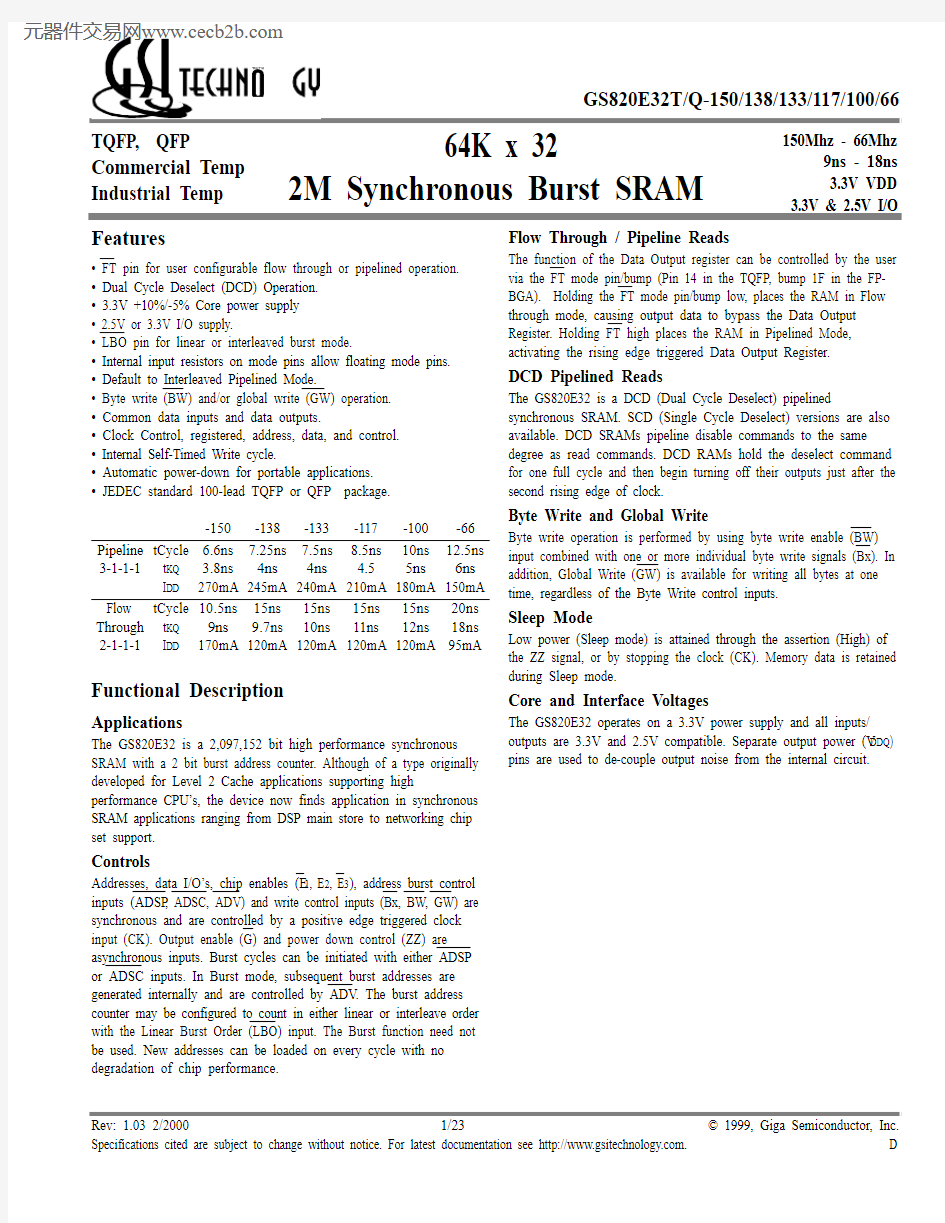
-150-138-133-117-100-66
3-1-1-1t KQ
I DD
3.8ns
270mA
4ns
245mA
4ns
240mA
4.5
210mA
5ns
180mA
6ns
150mA
Flow Through 2-1-1-1tCycle
t KQ
I DD
10.5ns
9ns
170mA
15ns
9.7ns
120mA
15ns
10ns
120mA
15ns
11ns
120mA
15ns
12ns
120mA
20ns
18ns
95mA
GS820E32 100 Pin TQFP and QFP Pinout
807978777675747372717069686766656463626160595857565554535251
123456789101112131415161718192021222324252627282930
V DDQ V SS DQ C4DQ C3V SS V DDQ DQ C2DQ C1
FT V DD NC V SS DQ D1DQ D2V DDQ V SS DQ D3DQ D4DQ D5V SS V DDQ V DDQ V SS DQ B4DQ B3V SS V DDQ DQ B2DQ B1V SS NC V DD ZZ DQ A1DQ A2V DDQ V SS DQ A3DQ A4V SS V DDQ L B O A 5
A 4
A 3
A 2
A 1
A 0
N C N C V S S
V D D
N C N C A 10
A 11
A 12
A 13
A 14
N C
A 6
A 7
E 1
E 2 B D
B C
B B
B A
E 3
C K G W B W V
D D
V S S
G A D S C A D S P A D V A 8
A 9
A 15
64K x 32Top View
DQ B5NC DQ B7DQ B8DQ B6DQ A6DQ A5DQ A8DQ A7NC
DQ C7DQ C8DQ C6DQ D6DQ D8DQ D7NC
DQ C5NC 10099989796959493929190898887868584838281
3132333435363738394041424344454647484950
TQFP Pin Description
E
Pin Location Symbol Type Description
37, 36A0, A1I Address field LSB’s and Address Counter preset Inputs 35, 34, 33, 32, 100, 99, 82, 81, 44, 45,
46, 47, 48, 49
A2-15I Address Inputs 52, 53, 56, 57, 58, 59, 62, 63
68, 69, 72, 73, 74, 75, 78, 79
2, 3, 6, 7, 8, 9, 12, 13
18, 19, 22, 23, 24, 25, 28, 29
DQ A1-DQ A8
DQ B1-DQ B8
DQ C1-DQ C8
DQ D1-DQ D8
I/O Data Input and Output pins.
16, 38, 39, 42, 43, 66, 50, 51, 80, 1, 30NC No Connect
87BW I Byte Write. Writes all enabled bytes. Active Low.
93, 94B A, B B I Byte Write Enable for DQ A, DQ B Data I/O’s. Active Low.
95, 96B C, B D I Byte Write Enable for DQ C, DQ D Data I/O’s. Active Low.
89CK I Clock Input Signal. Active High.
88GW I Global Write Enable. Writes all bytes. Active Low.
98, 92E1, E3I Chip Enable. Active Low.
97E2I Chip Enable. Active High.
86G I Output Enable. Active Low.
83ADV I Burst address counter advance enable. Active Low.
84, 85ADSP, ADSC I Address Strobe (Processor, Cache Controller). Active Low.
64ZZ I Sleep Mode control. Active High.
14FT I Flow Through or Pipeline mode. Active Low.
31LBO I Linear Burst Order mode. Active Low.
15, 41, 65, 91V DD I Core power supply.
5,10,17, 21, 26, 40, 55, 60, 67, 71, 76, 90V SS I I/O and Core Ground.
4, 11, 20, 27, 54, 61, 70, 77V DDQ I Output driver power supply.
GS820E18/32/36 Block Diagram
A1
A0
A0A1
D0
D1Q1Q0
Counter Load
D Q
D
Q
Register
Register
D
Q
Register
D
Q
Register
D
Q
Register
D Q
Register
D Q
Register
D Q
Register
D
Q
R e g i s t e r
D
Q
Register
A0-An LBO ADV CK ADSC ADSP GW BW B A
B B
B C
B D
E 1FT G
ZZ
Power Down Control
Memory Array
32
32
4
A
Q
D
E 2E 3
DQx1-DQx8
Note:
There are pull up devices on LBO and FT pins and a pull down device on and ZZ pin, so those input pins can be unconnected and the chip will operate in the default states as specified in the above tables.
Burst Counter Sequences
Byte Write Truth Table
Note:
1.All byte outputs are active in read cycles regardless of the state of Byte Write Enable inputs.
2.Byte Write Enable inputs B A , B B , B C and/or B D may be used in any combination with BW to write single or multiple bytes.
3.All byte I/O’s remain High-Z during all write operations regardless of the state of Byte Write Enable inputs.
Mode Pin Functions
Mode Name
Pin Name State
Function
Burst Order Control LBO L Linear Burst H or NC Interleaved Burst Output Register Control FT L Flow Through H or NC Pipeline Power Down Control
ZZ
L or NC Active H
Standby, I DD = I SB
Function
GW
BW
B A
B B
B C
B D
Notes
Read H H X X X X 1Read H L H H H H 1Write byte A H L L H H H 2, 3Write byte B H L H L H H 2, 3Write byte C H L H H L H 2, 3, 4Write byte D H L H H H L 2, 3, 4Write all bytes H L L L L L 2, 3, 4
Write all bytes
L
X
X
X
X
X
Linear Burst Sequence
Note: The burst counter wraps to initial state on the 5th clock.
I nterleaved Burst Sequence
Note: The burst counter wraps to initial state on the 5th clock.
A[1:0]
A[1:0]A[1:0]A[1:0]1st address 000110112nd address 011011003rd address 101100014th address
11
00
01
10
A[1:0]A[1:0]A[1:0]A[1:0]1st address 000110112nd address 010011103rd address 101100014th address
11
10
01
00
Synchronous Truth Table
Operation Address Used
State
Diagram
Key5
E1E2ADSP ADSC ADV W3DQ4
Deselect Cycle, Power Down None X H X X L X X High-Z Deselect Cycle, Power Down None X L F L X X X High-Z Deselect Cycle, Power Down None X L F H L X X High-Z Read Cycle, Begin Burst External R L T L X X X Q Read Cycle, Begin Burst External R L T H L X F Q Write Cycle, Begin Burst External W L T H L X T D Read Cycle, Continue Burst Next CR X X H H L F Q Read Cycle, Continue Burst Next CR H X X H L F Q Write Cycle, Continue Burst Next CW X X H H L T D Write Cycle, Continue Burst Next CW H X X H L T D Read Cycle, Suspend Burst Current X X H H H F Q Read Cycle, Suspend Burst Current H X X H H F Q Write Cycle, Suspend Burst Current X X H H H T D Write Cycle, Suspend Burst Current H X X H H T D Note:
1.X = Don’t Care, H = High, L = Low.
2. E = T (True) if E2 = 1 and E3 = 0; E = F (False) if E2 = 0 or E3 = 1.
3.W = T (True) and F (False) is defined in the Byte Write Truth Table preceding.
4.G is an asynchronous input. G can be driven high at any time to disable active output drivers. G low can only enable active drivers (shown
as “Q” in the Truth Table above).
5.All input combinations shown above are tested and supported. Input combinations shown in gray boxes need not be used to accomplish
basic synchronous or synchronous burst operations and may be avoided for simplicity.
6.Tying ADSP high and ADSC low allows simple non-burst synchronous operations. See BOLD items above.
7.Tying ADSP high and ADV low while using ADSC to load new addresses allows simple burst operations. See ITALIC items above.
First Write
First Read
Burst Write
Burst Read
Deselect
R W
CR
CW
X X
W
R
R
W
R
X
X
X S i m p l e S y n c h r o n o u s O p e r a t i o n
S i m p l e B u r s t S y n c h r o n o u s O p e r a t i o n
CR R
CW
CR
CR
Simplified State Diagram
Notes:
1.The diagram shows only supported (tested) synchronous state transitions. The diagram presumes G is tied Low.
2.The upper portion of the diagram assumes active use of only the Enable (E 1, E 2, E 3) and Write (B A , B B , B C , B D , BW and GW) control inputs
and that ADSP is tied high and ADSC is tied low.
3.The upper and lower portions of the diagram together assume active use of only the Enable, Write and ADSC control inputs and assumes
ADSP is tied high and ADV is tied low.
First Write
First Read
Burst Write
Burst Read
Deselect
R W
CR
CW
X
X
W
R
R
W
R
X
X
X CR
R CW CR
CR
W CW
W CW
Simplified State Diagram with G
Notes:
1.The diagram shows supported (tested) synchronous state transitions plus supported transitions that depend upon the use of G.
https://www.docsj.com/doc/6d1151220.html,e of “Dummy Reads” (Read Cycles with G High) may be used to make the transition from Read cycles to Write cycles without passing
through a Deselect cycle. Dummy Read cycles increment the address counter just like normal Read cycles.
3.Transitions shown in grey tone assume G has been pulsed high long enough to turn the RAM’s drivers off and for incoming data to meet
Data Input Set Up Time.
Absolute Maximum Ratings
(All voltages reference to V SS)
Symbol Description Value Unit
V DD Voltage on V DD Pins-0.5 to 4.6V
V DDQ Voltage in V DDQ Pins-0.5 to V DD V
V CK Voltage on Clock Input Pin-0.5 to 6V
V I/O Voltage on I/O Pins-0.5 to V DDQ+0.5 (≤ 4.6 V max.)V
V IN Voltage on Other Input Pins-0.5 to V DD+0.5 (≤ 4.6 V max.)V
I IN Input Current on Any Pin+/- 20mA
I OUT Output Current on Any I/O Pin+/- 20mA
P D Package Power Dissipation 1.5W
T STG Storage Temperature-55 to 125o C
T BIAS Temperature Under Bias-55 to 125o C
Note:
Permanent damage to the device may occur if the Absolute Maximum Ratings are exceeded. Operation should be restricted to Recommended Operating Conditions. Exposure to conditions exceeding the Absolute Maximum Ratings, for an extended period of time, may affect reliability of this component.
Recommended Operating Conditions
Parameter Symbol Min.Typ.Max.Unit Notes Supply Voltage V DD 3.135 3.3 3.6V
I/O Supply Voltage V DDQ 2.375 2.5V DD V1
Input High Voltage V IH 1.7---V DD+0.3V2
Input Low Voltage V IL-0.3---0.8V2 Ambient Temperature (Commercial Range Versions)T A02570°C3 Ambient Temperature (Industrial Range Versions)T A-402585°C3 Note:
1.Unless otherwise noted, all performance specifications quoted are evaluated for worst case at both
2.75V ≤ VDDQ ≤ 2.375V (i.e. 2.5V I/O)
and 3.6V ≤ VDDQ ≤ 3.135V (i.e. 3.3V I/O) and quoted at whichever condition is worst case.
2.This device features input buffers compatible with both
3.3V and 2.5V I/O drivers.
3.Most speed grades and configurations of this device are offered in both Commercial and Industrial Temperature ranges. The part number of
Industrial Temperature Range versions end the character “I”. Unless otherwise noted, all performance specifications quoted are evaluated for worst case in the temperature range marked on the device.
4.Input Under/overshoot voltage must be -2V > Vi < V DD+2V with a pulse width not to exceed 20% tKC.
Note: This parameter is sample tested.
Notes:
1.Junction temperature is a function of SRAM power dissipation, package thermal resistance, mounting board temperature, ambient. Temper-ature air flow, board density, and PCB thermal resistance.
2.SCMI G-38-87.
3.Average thermal resistance between die and top surface, MIL SPEC-883, Method 1012.1.
Capacitance
(T A =25o C, f=1MH Z , V DD =3.3V)
Parameter
Symbol
Test conditions
Typ.
Max.
Unit
Control Input Capacitance C I V DD =3.3V 34pF Input Capacitance C IN V IN =0V 45pF Output Capacitance
C OUT
V OUT =0V
6
7
pF
Package Thermal Characteristics
Rating
Layer Board
Symbol
TQFP Max
QFP Max
Unit
Notes
Junction to Ambient (at 200 lfm)single R ΘJA 40TBD °C/W 1,2,4Junction to Ambient (at 200 lfm)four
R ΘJA 24TBD °C/W 1,2,4Junction to Case (TOP)
R ΘJC
9
TBD
°C/W
3,4
20% tKC
V SS -2.0V
50%V SS V IH
Undershoot Measurement and Timing
Overshoot Measurement and Timing
20% tKC
V DD +-2.0V
50%V DD
V IL
Notes:
1.Include scope and jig capacitance.
2.Test conditions as specified with output loading as shown in Fig. 1 unless otherwise noted.
3.Output Load 2 for t LZ , t HZ , t OLZ and t OHZ .
4.Device is deselected as defined by the Truth Table.
AC Test Conditions
Parameter
Conditions
Input high level 2.3V Input low level 0.2V Input slew rate 1V/ns Input reference level 1.25V Output reference level
1.25V
Output load Fig. 1& 2DC Electrical Characteristics
Parameter
Symbol
Test Conditions
Min
Max
Input Leakage Current (except mode pins)I IL V IN = 0 to V DD -1uA 1uA ZZ Input Current I INZZ V DD ≥ V IN ≥ V IH 0V ≤ V IN ≤ V IH -1uA -1uA 1uA 300uA Mode Pin Input Current I INM V DD ≥ V IN ≥ V IL 0V ≤ V IN ≤ V IL -300uA -1uA 1uA 1uA Output Leakage Current I OL Output Disable,V OUT = 0 to V DD -1uA 1uA
Output High Voltage V OH I OH = - 4mA, V DDQ =2.375V 1.7V Output High Voltage V OH I OH = - 4mA, V DDQ =3.135V
2.4V
Output Low Voltage
V OL
I OL = 4mA
0.4V
DQ
VT=1.25V
50?30pF *
DQ
2.5V
Output Load 1
Output Load 2
225?225?
5pF *
* Distributed Test Jig Capacitance
Operating Currents
Operating Currents
Parameter
Test Conditions
Symbol
-150
-138
-133
0 to 70°C -40 to 85°C
0 to 70°C -40 to 85°C 0 to 70°C -40 to 85°C Operating Current Device Selected; All other inputs ≥V IH o r ≤ V IL Output open I DD Pipeline 270mA 275mA 245mA 250mA 240mA 245mA I DD Flow-Thru 170mA 175mA 120mA 125mA 120mA 125mA Standby Current ZZ ≥ V DD - 0.2V I SB Flow-Thru 10mA 15mA 10mA 15mA 10mA 15mA Deselect Current
Device Deselected; All other inputs ≥ V IH or ≤ V IL
I DD Pipeline 90mA 95mA 80mA 85mA 80mA 85mA I DD Flow-Thru
45mA
50mA
40mA
45mA
40mA
45mA
Parameter
Test Conditions
Symbol
-117
-100
-66
0 to 70°C -40 to 85°C 0 to 70°C -40 to 85°C 0 to 70°C -40 to 85°C Operating Current Device Selected; All other inputs ≥V IH o r ≤ V IL Output open I DD Pipeline 210mA 215mA 180mA 185mA 150mA 155mA I DD Flow-Thru 120mA 125mA 120mA 125mA 95mA 100mA Standby Current ZZ ≥ V DD - 0.2V I SB Flow-Thru 10mA 15mA 10mA 15mA 10mA 15mA Deselect Current
Device Deselected; All other inputs ≥ V IH or ≤ V IL
I DD Pipeline 70mA 75mA 60mA 65mA 50mA 55mA I DD Flow-Thru
40mA
45mA
40mA
45mA
40mA
45mA
AC Electrical Characteristics
Notes:
1.These parameters are sampled and are not 100% tested
2.ZZ is an asynchronous signal. However, In order to be recognized on any given clock cycle, ZZ must meet the specified setup and hold
times as specified above.
Parameter
Symbol
-150
-138
-133
-117
-100
-66
Unit
Min Max Min Max Min Max Min Max Min Max
Min Max
Pipeline
Clock Cycle Time
tKC 6.6---7.25---7.5---8.5---10
12.5
ns Clock to Output Valid tKQ --- 3.8---4---4--- 4.55
6ns Clock to Output Invalid tKQX 1.5---2---2---2---22ns Clock to Output in Low-Z tLZ 1 1.5---2---2---2---2
2ns Flow-Thru
Clock Cycle Time
tKC 10.5---15---15---15---15
20ns
Clock to Output Valid tKQ ---9.0---9.7---10---1112
18ns Clock to Output Invalid tKQX 3---3---3---3---33ns Clock to Output in Low-Z tLZ 13---3---3---3---33ns Clock HIGH Time tKH 1.8--- 1.9--- 1.9---2---34ns Clock LOW Time tKL 1.8--- 1.9--- 1.9---2---34ns
Clock to Output in High-Z
tHZ 1 1.5 3.8 1.54 1.5 4 1.5456ns G to Output Valid tOE --- 3.8---4---4---45
6
ns G to output in Low-Z tOLZ 10---0---0---0---00ns
G to output in High-Z
tOHZ 1---4---4---4---45
6ns Setup time tS 1.7---2---2---2---22ns Hold time tH 0.5---0.5---0.5---0.5---0.50.5ns ZZ setup time tZZS 25---5---5---5---55ns ZZ hold time tZZH 21---1---1---1---11ns ZZ recovery
tZZR
20
---
20
---
20
---
20
---20
20
ns
CK ADSP ADSC ADV
GW BW
G
WR2WR3 WR1
WR1WR2WR3
tKC
Single Write
Burst Write
D2A D2B D2C D2D D3A
D1A
t KL
t KH
tS tH
tS tH
tS tH
tS tH
tS tH
tS tH
tS tH
tS tH Write specified byte for 2A and all bytes for 2B, 2C& 2D
ADV must be inactive for ADSP Write
ADSC initiated write
ADSP is blocked by E1 inactive
A0-An
B A - B D DQ A - DQ D
Write Deselected Hi-Z
WR1WR3
Write Cycle Timing
E1 E3tS tH
tS tH
tS tH
E2 and E3 only sampled with ADSP or ADSC
E1 masks ADSP
E2
Deselected with E2
Q 1A
Q 3A
Q 2D
Q 2C
Q 2B
Q 2A
tKQ
tLZ tOE
tOHZ
tOLZ
tKQX
tHZ
tKQX
CK
ADSP ADSC
BW G
GW
ADV
Burst Read
RD2RD3
tKL
tS
tH
tH
tS tH
tS tH
ADSC initiated read
Suspend Burst Single Read
ADSP is blocked by E 1 inactive
A 0-An
B A - B D
tKH
tKC
tS tH
tS tS
tH
DQ A -DQ D
RD1
Hi-Z
Suspend Burst
Flow Through Read Cycle Timing
E 2
tS tH
tH
tH
E 1 masks ADSP
E 2 and E 3 only sampled with ADSP or ADSC
Deselected with E 2
E 3
E 1
tS tS
Flow Through Read-Write Cycle Timing
CK
ADSP
ADSC
ADV
GW
BW G
RD1WR1RD2
Q1A
D1A
Q2A
Q2B
Q2C
Q2D
Single Read
Burst Read
tOE
tOHZ
tS tH
tS
tH
tH
tS tH
tS tH
tS tH
tS tH
tKH ADSC initiated read
DQ A - DQ D
B A - B D
A0-An tKL
tKC
tS Single Write
ADSP is blocked by E inactive
tKQ
tS
tH
Hi-Z
Q2A
Burst wrap around to it’s initial state
WR1
E 1
E 3
E 2
tS tS tH
tS E1 masks ADSP
E2 and E3 only sampled with ADSP and ADSC
Deselected with E3
tH
tH
Pipelined DCD Read Cycle Timing
Q1a
Q3A
Q2D
Q2C
Q2B
Q2A
tKQ
tLZ
tOE
tOHZ
tOLZ
tKQX tHZ
tKQX CK
ADSP ADSC
BW G
GW
ADV
E 2
Burst Read
RD2RD3
tKL
tS tH
tH
tH
tS
tH
tH
tS tH
tS tH
ADSC initiated read
Suspend Burst
E 1 masks ADSP
E 2 and E 3 only sampled with ADSP or ADSC
Deselected with E 2
Single Read
ADSP is blocked by E 1 inactive
A 0-An
B A - B D
E 3
E 1
tKH tKC
tS tH
tS tS
tH
DQ A -DQ D
tS tS RD1
Hi-Z
Pipelined DCD Read-Write Cycle Timing
CK
ADSP
ADV
GW
BW
E 1
E 3G
E 2
WR1
Q1A
D1A
Q2A Q2B Q2C Q2D
Single Read
Burst Read
tOE
tOHZ
tS tS tH
tS tS tH
tS tH
tH
tS tH
tS tH
tKH
E 1 masks ADSP
E 2 and E 3 only sampled with ADSP and ADSC
Deselected with E 3
DQ A - DQ D
tKL
tKC tS tH
tH
Single Write
ADSP is blocked by E 1 inactive
tKQ
tS tH
Hi-Z
B A - B D
RD1WR1RD2
tS tH
A 0-A n
ADSC
tS tH
ADSC initiated read
Application Tips
Single and Dual Cycle Deselect
SCD devices force the use of “dummy read cycles” (read cycles that are launched normally but that are ended with the output drivers inactive) in
a fully synchronous environment. Dummy read cycles waste performance but their use usually assures there will be no bus contention in
transitions from reads to writes or between banks of RAMs. DCD SRAMs do not waste bandwidth on dummy cycles and are logically simpler to manage in a multiple bank application (wait states need not be inserted at bank address boundary crossings) but greater care must be exercised to avoid excessive bus contention.
CK
ADSP ADSC
tH
tKH tKL
tKC
tS ZZ
tZZR
tZZH
tZZS
~~~~
~~~~~Snooze
Sleep Mode Timing Diagram
E