MAX4175BCEUK-T中文资料
For free samples & the latest literature: https://www.docsj.com/doc/5013769071.html,, or phone 1-800-998-8800.For small orders, phone 1-800-835-8769.
General Description
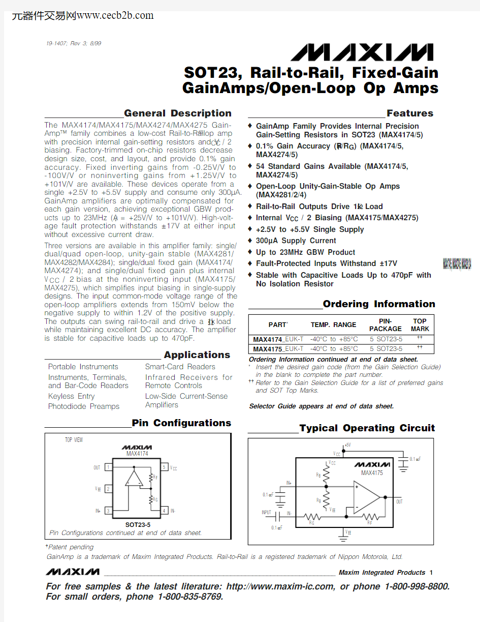
The MAX4174/MAX4175/MAX4274/MAX4275 Gain-Amp? family combines a low-cost Rail-to-Rail ?op amp with precision internal gain-setting resistors and V CC / 2biasing. Factory-trimmed on-chip resistors decrease design size, cost, and layout, and provide 0.1% gain accuracy. Fixed inverting gains from -0.25V/V to -100V/V or noninverting gains from +1.25V/V to +101V/V are available. These devices operate from a single +2.5V to +5.5V supply and consume only 300μA.GainAmp amplifiers are optimally compensated for each gain version, achieving exceptional GBW prod-ucts up to 23MHz (A V = +25V/V to +101V/V). High-volt-age fault protection withstands ±17V at either input without excessive current draw.
Three versions are available in this amplifier family: single/dual/quad open-loop, unity-gain stable (MAX4281/MAX4282/MAX4284); single/dual fixed gain (MAX4174/MAX4274); and single/dual fixed gain plus internal V CC / 2bias at the noninverting input (MAX4175/MAX4275), which simplifies input biasing in single-supply designs. The input common-mode voltage range of the open-loop amplifiers extends from 150mV below the negative supply to within 1.2V of the positive supply.The outputs can swing rail-to-rail and drive a 1k ?load while maintaining excellent DC accuracy. The amplifier is stable for capacitive loads up to 470pF.
Applications
Portable Instruments Smart-Card Readers
Instruments, Terminals, Infrared Receivers for and Bar-Code Readers Remote Controls
Keyless Entry
Low-Side Current-Sense Photodiode Preamps
Amplifiers
Features
o GainAmp Family Provides Internal Precision Gain-Setting Resistors in SOT23 (MAX4174/5)o 0.1% Gain Accuracy (R F /R G ) (MAX4174/5,MAX4274/5)o 54 Standard Gains Available (MAX4174/5,MAX4274/5)o Open-Loop Unity-Gain-Stable Op Amps (MAX4281/2/4)o Rail-to-Rail Outputs Drive 1k ?Load
o Internal V CC / 2 Biasing (MAX4175/MAX4275)o +2.5V to +5.5V Single Supply o 300μA Supply Current o Up to 23MHz GBW Product
o Fault-Protected Inputs Withstand ±17V o Stable with Capacitive Loads Up to 470pF with No Isolation Resistor
MAX4174/5, MAX4274/5, MAX4281/2/4?
SOT23, Rail-to-Rail, Fixed-Gain GainAmps/Open-Loop Op Amps
________________________________________________________________Maxim Integrated Products
1
19-1407; Rev 3; 8/99
Ordering Information continued at end of data sheet.
*Insert the desired gain code (from the Gain Selection Guide)in the blank to complete the part number.
??Refer to the Gain Selection Guide for a list of preferred gains and SOT Top Marks.Ordering Information
GainAmp is a trademark of Maxim Integrated Products. Rail-to-Rail is a registered trademark of Nippon Motorola, Ltd.
?Patent pending
Pin Configurations
Typical Operating Circuit
Selector Guide appears at end of data sheet.
M A X 4174/5, M A X 4274/5, M A X 4281/2/4
SOT23, Rail-to-Rail, Fixed-Gain GainAmps/Open-Loop Op Amps 2_______________________________________________________________________________________
ABSOLUTE MAXIMUM RATINGS
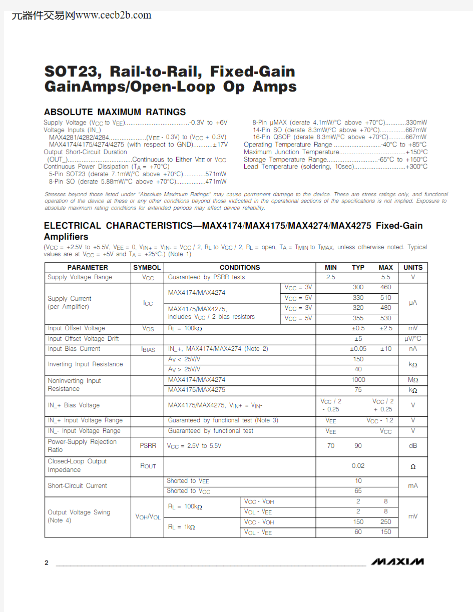
ELECTRICAL CHARACTERISTICS—MAX4174/MAX4175/MAX4274/MAX4275 Fixed-Gain Amplifiers
(V CC = +2.5V to +5.5V, V EE = 0, V IN+= V IN-= V CC / 2, R L to V CC / 2, R L = open, T A = T MIN to T MAX , unless otherwise noted. Typical values are at V CC = +5V and T A = +25°C.) (Note 1)
Stresses beyond those listed under “Absolute Maximum Ratings” may cause permanent damage to the device. These are stress ratings only, and functional operation of the device at these or any other conditions beyond those indicated in the operational sections of the specifications is not implied. Exposure to absolute maximum rating conditions for extended periods may affect device reliability.
Supply Voltage (V CC to V EE )....................................-0.3V to +6V Voltage Inputs (IN_)
MAX4281/4282/4284.....................(V EE - 0.3V) to (V CC + 0.3V)MAX4174/4175/4274/4275 (with respect to GND)...........±17V Output Short-Circuit Duration
(OUT_).....................................Continuous to Either V EE or V CC Continuous Power Dissipation (T A = +70°C)
5-Pin SOT23 (derate 7.1mW/°C above +70°C).............571mW 8-Pin SO (derate 5.88mW/°C above +70°C).................471mW
8-Pin μMAX (derate 4.1mW/°C above +70°C)............330mW 14-Pin SO (derate 8.3mW/°C above +70°C)...............667mW 16-Pin QSOP (derate 8.3mW/°C above +70°C)..........667mW Operating Temperature Range ...........................-40°C to +85°C Maximum Junction Temperature.....................................+150°C Storage Temperature Range.............................-65°C to +150°C Lead Temperature (soldering, 10sec).............................+300°C
ELECTRICAL CHARACTERISTICS—MAX4174/MAX4175/MAX4274/MAX4275 Fixed-Gain
MAX4174/5, MAX4274/5, MAX4281/2/4SOT23, Rail-to-Rail, Fixed-Gain GainAmps/Open-Loop Op Amps Amplifiers (continued)
= +2.5V to +5.5V, V= 0, V= V= V/ 2, R to V/ 2, R= open, T= T to T, unless otherwise noted. Typical
(V
ELECTRICAL CHARACTERISTICS—MAX4281/MAX4282/MAX4284 Open-Loop Op Amps (V CC= +2.5V to +5.5V, V EE= 0, V IN+= V IN-= V CC/ 2, R L to V CC/ 2, R L= open, T A= T MIN to T MAX, unless otherwise noted. Typical
values are at V CC= +5V and T A= +25°C.) (Note 1)
Typical Operating Characteristics
(V CC = +5V, R L = 100k ?to V CC / 2, small-signal V OUT = 100mVp-p, large-signal V OUT = 1Vp-p, T A = +25°C, unless otherwise noted.)
M A X 4174/5, M A X 4274/5, M A X 4281/2/4
SOT23, Rail-to-Rail, Fixed-Gain GainAmps/Open-Loop Op Amps 4_______________________________________________________________________________________
Note 1:MAX4174/MAX4175/MAX4281 and MAX4274/MAX4275/MAX4282 and MAX4284 are 100% production tested at
T A = +25°C. All temperature limits are guaranteed by design.
Note 2:Guaranteed by design.
Note 3:The input common-mode range for IN_+ is guaranteed by a functional test. A similar test is done on the IN_- input. See the
Applications Information section for more information on the input voltage range of the GainAmp.
Note 4:For A V = -0.5V/V and A V = -0.25V/V, the output voltage swing is limited by the input voltage range.Note 5:Includes noise from on-chip resistors.
Note 6:The gain accuracy test is performed with the GainAmp in noninverting configuration. The output voltage swing is limited by
the input voltage range for certain gains and supply voltage conditions. For situations where the output voltage swing is lim-ited by the valid input range, the output limits are adjusted accordingly.
4-6
1k
100k 1M
10k
10M
LARGE-SIGNAL GAIN vs. FREQUENCY
FREQUENCY (Hz)
N O R M A L I Z E D G A I N (d B )
-5-4-3-2-101234-6
1k
100k 1M
10k
10M
LARGE-SIGNAL GAIN vs. FREQUENCY
FREQUENCY (Hz)
N O R M A L I Z E D G A I N (d B )
-5
-4-3-2-101234
-6
1k 100k 1M 10k 10M
LARGE-SIGNAL GAIN
vs. FREQUENCY
FREQUENCY (Hz)
N O R M A L I Z E D G A I N (d B )
-5-4-3-2-10123
ELECTRICAL CHARACTERISTICS—MAX4281/MAX4282/MAX4284 Open-Loop Op Amps (continued)
(V CC = +2.5V to +5.5V, V EE = 0, V IN+= V IN-= V CC / 2, R L to V CC / 2, R L = open, T A = T MIN to T MAX , unless otherwise noted. Typical values are at V = +5V and T = +25°C.) (Note 1)
MAX4174/5, MAX4274/5, MAX4281/2/4
SOT23, Rail-to-Rail, Fixed-Gain GainAmps/Open-Loop Op Amps
_______________________________________________________________________________________5
Typical Operating Characteristics (continued)
(V CC = +5V, R L = 100k ?to V CC / 2, small-signal V OUT = 100mVp-p, large-signal V OUT = 1Vp-p, T A = +25°C, unless otherwise noted.)
4-6
1k
100k 1M
10k
10M
LARGE-SIGNAL GAIN vs. FREQUENCY
FREQUENCY (Hz)
N O R M A L I Z E D G A I N (d B )
-5-4-3-2-101234-6
1k
100k 1M
10k
10M
LARGE-SIGNAL GAIN vs. FREQUENCY
FREQUENCY (Hz)
N O R M A L I Z E D G A I N (d B )
-5
-4-3-2-101234
-6
1k 100k 1M 10k 10M
LARGE-SIGNAL GAIN vs. FREQUENCY
FREQUENCY (Hz)
N O R M A L I Z E D G A I N (d B )
-5-4-3-2-101234-6
1k
100k 1M
10k
10M
SMALL-SIGNAL GAIN vs. FREQUENCY
FREQUENCY (Hz)
N O R M A L I Z E D G A I N (d B )
-5-4-3-2-101234-6
1k
100k 1M
10k
10M
SMALL-SIGNAL GAIN
vs. FREQUENCY
FREQUENCY (Hz)
N O R M A L I Z E D G A I N (d B )
-5
-4-3-2-101234
-6
1k 100k 1M 10k 10M
SMALL-SIGNAL GAIN
vs. FREQUENCY
FREQUENCY (Hz)
N O R M A L I Z E D G A I N (d B )
-5-4-3-2-10123MAX4174/MAX4175
4-6
1k
100k 1M
10k
10M SMALL-SIGNAL GAIN vs. FREQUENCY
FREQUENCY (Hz)
N O R M A L I Z E D G A I N (d B )
-5-4-3-2-101234-6
1k 100k 1M 10k 10M SMALL-SIGNAL GAIN vs. FREQUENCY
FREQUENCY (Hz)
N O R M A L I Z E D G A I N (d B )
-5-4-3-2-101234
-6
1k 100k 1M 10k 10M
SMALL-SIGNAL GAIN vs. FREQUENCY
FREQUENCY (Hz)
N O R M A L I Z E D G A I N (d B )
-5-4-3-2-10123
M A X 4174/5, M A X 4274/5, M A X 4281/2/4
SOT23, Rail-to-Rail, Fixed-Gain GainAmps/Open-Loop Op Amps 6_______________________________________________________________________________________
1k
10k
100k
1M
TOTAL HARMONIC DISTORTION
vs. FREQUENCY
FREQUENCY (Hz)
T H D (d B )
0-120
-100
-80-60-40-20
1k
10k
100k
1M
TOTAL HARMONIC DISTORTION
vs. FREQUENCY
FREQUENCY (Hz)
T H D (d B )
0-120
-100
-80-60-40-20
-120
-90
-100
-110-80-70-600
2.01.50.5 1.0 2.5
3.0 3.5
4.0 4.5
5.0
TOTAL HARMONIC DISTORTION vs. OUTPUT VOLTAGE SWING
VOLTAGE SWING (Vp-p)
T H D (d B )
Typical Operating Characteristics (continued)
(V CC = +5V, R L = 100k ?
to V CC / 2, small-signal V OUT = 100mVp-p, large-signal V OUT = 1Vp-p, T A = +25°C, unless otherwise noted.)
MAX4174/MAX4175
-120
-90
-100-110-80-70-600
2.01.50.5 1.0 2.5
3.0 3.5
4.0 4.5
5.0
TOTAL HARMONIC DISTORTION vs. OUTPUT VOLTAGE SWING
VOLTAGE SWING (Vp-p)
T H D (d B )
1
10
100
1k
10k
100k
VOLTAGE NOISE DENSITY vs. FREQUENCY
(A V = +1.25, +3, +10)
FREQUENCY (Hz)
100010
100
V O L T A G E N O I S E D E N S I T Y (n V /H z )
1
10
100
1k
10k
100k
VOLTAGE NOISE DENSITY vs. FREQUENCY
(A V = +25, +51)
FREQUENCY (Hz)
100010
100
V O L T A G E N O I S E D E N S I T Y (n V /√H z )
1
10
100
1k
10k
100k
CURRENT NOISE DENSITY vs.
FREQUENCY
M A X 4174/5 t o c 19
FREQUENCY (Hz)
101
C U R R E N T N O I S E
D
E N S I T Y (f A /√H z )
MAX4174/5, MAX4274/5, MAX4281/2/4
SOT23, Rail-to-Rail, Fixed-Gain GainAmps/Open-Loop Op Amps
_______________________________________________________________________________________7
Typical Operating Characteristics (continued)
(V CC = +5V, R L = 100k ?to V CC / 2, small-signal V OUT = 100mVp-p, large-signal V OUT = 1Vp-p, T A = +25°C, unless otherwise noted.)
2μs/div
C L = 0
INPUT VOLTAGE
A V = +1.25V/V
OUTPUT 500mV/div
A V = +3V/V OUTPUT 50mV/div
A V = +5V/V OUTPUT 500mV/div
A V = +10V/V OUTPUT 500mV/div
A V = +25V/V OUTPUT 500mV/div
A V = +51V/V OUTPUT 500mV/div
M A X 4174/5 t o c 20
LARGE-SIGNAL PULSE RESPONSE
2μs/div
C L = 0
INPUT VOLTAGE
A V = +1.25V/V
OUTPUT 50mV/div
A V = +3V/V OUTPUT 50mV/div
A V = +5V/V OUTPUT 50mV/div
A V = +10V/V OUTPUT 50mV/div
A V = +25V/V OUTPUT 50mV/div
A V = +51V/V OUTPUT 50mV/div
M A X 4174/5 t o c 21
SMALL-SIGNAL PULSE RESPONSE
MAX4174/MAX4175
M A X 4174/5, M A X 4274/5, M A X 4281/2/4
SOT23, Rail-to-Rail, Fixed-Gain GainAmps/Open-Loop Op Amps 8_______________________________________________________________________________________
Typical Operating Characteristics (continued)
(V CC = +5V, R L = 100k ?to V CC / 2, small-signal V OUT = 100mVp-p, large-signal V OUT = 1Vp-p, T A = +25°C, unless otherwise noted.)
-200
-100-150500-50150100200-50-5
10
-35-20
25
40
55
70
85INPUT OFFSET VOLTAGE vs.
TEMPERATURE
TEMPERATURE (°C)I N P U T O F F S E T V O L T A G E (μV )
-200
02004006008001000-45-15-300153045607590
INPUT BIAS CURRENT vs. TEMPERATURE
TEMPERATURE (°C)
I N P U T B I A S C U R R E N T (p A )240
280260320300360340380-50-20
-5
-3510
25
40
55
70
85SUPPLY CURRENT vs. TEMPERATURE
TEMPERATURE (°C)S U P P L Y C U R R E N T (μA )
-100
-60-80-20-40200408060100-50-20-510-352540557085
V OH AND V OL vs. TEMPERATURE
(V CC = 2.5V)
TEMPERATURE (°C)V O L T A G E (m V )
-100
-60-40-20-80406002080100160180120140200-50-20
-5
10
-3525
40
55
70
85
V OH AND V OL vs. TEMPERATURE
(V CC = 5.5V)
TEMPERATURE (°C)
V O L T A G E (m V )
MAX4174/MAX4175/MAX4281/MAX4282/MAX4284
-70100
10k 100k
1k
1M
POWER-SUPPLY REJECTION
vs. FREQUENCY
M A X 4174 T O C 22
FREQUENCY (Hz)
P S R (d B )
-95-90
-85-80
-75
100
10k 100k
1k
1M
OUTPUT IMPEDANCE vs. FREQUENCY
M A X 4174 T O C 23
FREQUENCY (Hz)
O U T P U T I M P E D A N C E (?)
1000.01
0.11
10
5.0
4.0
1
10100
OUTPUT VOLTAGE SWING
vs. R LOAD
M A X 4174 T O C 24
R LOAD (k ?)
V S W I N G (V p -p )
4.94.84.74.64.54.44.3
4.24.1
MAX4174/5, MAX4274/5, MAX4281/2/4
SOT23, Rail-to-Rail, Fixed-Gain GainAmps/Open-Loop Op Amps
_______________________________________________________________________________________9
110k 1M
100101k 100k 10M
OPEN-LOOP GAIN AND PHASE
vs. FREQUENCY
M A X 4174/5 t o c 30
FREQUENCY (Hz)
O P E N -L O O P G A I N (d B )
P H A S E (d e g r e e s )
1401201008060400-20-40
20160-45-90-135-180-225-270-31504-6-51k
10k
100k 1M
10M SMALL-SIGNAL GAIN vs. FREQUENCY
-4-3M A X 4174/5 t o c 31
FREQUENCY (Hz)
G A I N (d B )
-2-1012
34
-1-2-3-4-5-6
1k 10k 100k 1M 10M
LARGE-SIGNAL GAIN vs. FREQUENCY
0M A X 4174/5 t o c 32
FREQUENCY (Hz)
G A I N (d B )
1230-50-60-70-80-90-100
1k
10k
100k
100
1M
10M
COMMON-MODE REJECTION
vs. FREQUENCY
-40M A X 4174/5 t o c 33
FREQUENCY (Hz)
C M R (d B
)-30-20-100-60-80-70-90-100-110-10-20-30-40-50-120
1M
1k
10k
100k
TOTAL HARMONIC DISTORTION
vs. FREQUENCY
FREQUENCY (Hz)
T H D (d B )
1000100
10
10
100
1k
1
10k
100k
VOLTAGE NOISE DENSITY
vs. FREQUENCY
M A X 4174/5 t o c 34
FREQUENCY (Hz)
V O L T A G E N O I S E D E N S I T Y (n V /√H z )
101101001k 1
10k 100k
CURRENT NOISE DENSITY
vs. FREQUENCY
M A X 4174/5 t o c 35
FREQUENCY (Hz)
C U R R E N T N O I S E
D
E N S I T Y (f A /√H z )
-50-80-90-85-95
-55-60-65-70-751M
10M
1k
10k
100k MAX4282
CROSSTALK vs. FREQUENCY
M A X 4174/5 t o c 37
FREQUENCY (Hz)
C R O
S S T A L K (d B )
-50
-55-60
-65
-70-75
1M
10M
1k
10k
100k MAX4284
CROSSTALK vs. FREQUENCY
FREQUENCY (Hz)
C R O S S T A L K (d B )
Typical Operating Characteristics
(V CC = +5V, R L = 100k ?to V CC / 2, small-signal V OUT = 100mVp-p, large-signal V OUT = 1Vp-p, T A = +25°C, unless otherwise noted.)
MAX4281/MAX4282/MAX4284
M A X 4174/5, M A X 4274/5, M A X 4281/2/4
SOT23, Rail-to-Rail, Fixed-Gain GainAmps/Open-Loop Op Amps 10______________________________________________________________________________________
Functional Diagrams
Pin Description
Detailed Description Maxim’s GainAmp fixed-gain amplifiers combine a low-cost rail-to-rail op amp with internal gain-setting resis-tors. Factory-trimmed on-chip resistors provide 0.1% gain accuracy while decreasing design size, cost, and layout. Three versions are available in this amplifier family: single/dual/quad open-loop, unity-gain-stable devices (MAX4281/MAX4282/MAX4284); single/dual fixed-gain devices (MAX4174/MAX4274); and single/ dual devices with fixed gain plus internal V CC / 2 bias at the noninverting input (MAX4175/MAX4275). All amplifiers feature rail-to-rail outputs and drive a 1k?load while maintaining excellent DC accuracy.
Open-Loop Op Amps The single/dual/quad MAX4281/MAX4282/MAX4284 are high-performance, open-loop op amps with rail-to-rail outputs. These devices are compensated for unity-gain stability, and feature a gain bandwidth (GBW) of 2MHz. The op amps in these ICs feature an input com-mon-mode range that extends from 150mV below the negative rail to within 1.2V of the positive rail. These high performance op amps serve as the core for this family of GainAmp fixed-gain amplifiers. Although the -3dB bandwidth will not correspond to that of a fixed-gain amplifier in higher gain configurations, these open-loop op-amps can be used to prototype designs.
Internal Gain-Setting Resistors Maxim’s proprietary laser trimming techniques produce the necessary R F/R G values (Figure 1), so many gain offerings are easily available. These GainAmp fixed-gain amplifiers feature a negative-feedback resistor network that is laser trimmed to provide a gain-setting feedback ratio (R F/R G) with 0.1% typical accuracy. The standard op amp pinouts allow the GainAmp fixed-gain amplifiers to drop in directly to existing board designs, easily replacing op-amp-plus-resistor gain blocks.
GainAmp Bandwidth GainAmp fixed-gain amplifiers feature factory-trimmed precision resistors to provide fixed inverting gains from -0.25V/V to -100V/V or noninverting gains from +1.25V/V to +101V/V. The op-amp core is decompen-sated strategically over the gain-set options to maxi-mize bandwidth. Open-loop decompensation increases GBW product, ensuring that usable bandwidth is main-tained with increasing closed-loop gains. A GainAmp with a fixed gain of A V= 100V/V has a -3dB bandwidth of 230kHz. By comparison, a unity-gain-stable op amp configured for A V= 100V/V would yield a -3dB band-width of only 20kHz (Figure 2). Decompensation is per-formed at five intermediate gain sets, as shown in the Gain Selection Guide. Low gain decompensation great-ly increases usable bandwidth, while decompensation above gains of +25V/V offers diminished returns.
V CC / 2 Internal Bias The MAX4175/MAX4275 GainAmp fixed-gain amplifiers with the V CC / 2 bias option are identical to standard GainAmp fixed-gain amplifiers, with the added feature of V CC / 2 internal bias at the noninverting inputs. Two 150k?resistors form a voltage-divider for self-biasing the noninverting input, eliminating external bias resis-tors for AC-coupled applications, and allowing maxi-mum signal swing at the op amp’s rail-to-rail output for single-supply systems (see Typical Operating Circuit). For DC-coupled applications, use the MAX4174/ MAX4274.
High-Voltage (±17V) Input Fault Protection The MAX4174/MAX4175/MAX4274/MAX4275 include ±17V input fault protection. For normal operation, see the input voltage range specification in the Electrical Characteristics. Overdriven inputs up to ±17V will not
Figure 1. Internal Gain-Setting Resistors
Figure 2. Gain-Bandwidth Comparison
MAX4174/5, MAX4274/5, MAX4281/2/4SOT23, Rail-to-Rail, Fixed-Gain GainAmps/Open-Loop Op Amps
______________________________________________________________________________________11
M A X 4174/5, M A X 4274/5, M A X 4281/2/4
SOT23, Rail-to-Rail, Fixed-Gain GainAmps/Open-Loop Op Amps 12______________________________________________________________________________________
cause output phase reversal. A back-to-back SCR structure at the input pins allows either input to safely swing ±17V relative to V EE (Figure 3). Additionally, the internal op-amp inputs are diode clamped to either supply rail for the protection of sensitive input stage cir-cuitry. Current through the clamp diodes is limited by a 5k ?resistor at the noninverting input, and by R G at the inverting input. An IN+ or IN- fault voltage as high as ±17V will cause less than 3.5mA of current to flow through the input pin, protecting both the GainAmp and the signal source from damage.
Applications Information
GainAmp fixed-gain amplifiers offer a precision, fixed gain amplifier in a small package that can be used in a variety of circuit board designs. GainAmp fixed-gain amplifiers can be used in many op amp circuits that use resistive negative feedback to set gain, and that do not require other connections to the op-amp inverting input.Both inverting and noninverting op-amp configurations can be implemented easily using a GainAmp.
GainAmp Input Voltage Range
The MAX4174/MAX4175/MAX4274/MAX4275 combine both an op amp and gain-setting feedback resistors on the same chip. Because the inverting input pin is actu-ally tied to the R G input series resistor, the inverting input voltage range is different from the noninverting input voltage range. Just as with a discrete design,care must be taken not to saturate the inputs/output of the core op amp, to avoid signal distortions or clipping.The inverting inputs (IN_-) of the MAX4174/MAX4175/MAX4274/MAX4275 must be within the supply rails or signal distortion may result. The GainAmp’s inverting input structure includes diodes to both supplies, such that driving the inverting input beyond the rails may cause signal distortions (Figure 1). For applications that require sensing voltages beyond the rails, use the MAX4281/MAX4282/MAX4284 open-loop op amps (Figure 4).
Figure 3. Input Protection
MAX4174/5, MAX4274/5, MAX4281/2/4
SOT23, Rail-to-Rail, Fixed-Gain GainAmps/Open-Loop Op Amps
______________________________________________________________________________________13
GainAmp Signal Coupling
and Configurations
Common op-amp configurations include both nonin-verting and inverting amplifiers. Figures 5–8 show vari-ous single and dual-supply circuit configurations.Single-supply systems benefit from a midsupply bias on the noninverting input (provided internally on MAX4175/MAX4275), as this produces a quiescent DC level at the center of the rail-to-rail output stage signal swing. For dual-supply systems, ground-referenced signals may be DC-coupled into the inverting or non-inverting inputs.
IN_+ Filter on MAX4175/MAX4275
Internal resistor biasing of the V CC / 2 bias options cou-ples power-supply noise directly to the op amp’s nonin-verting input. To minimize high-frequency power-supply noise coupling, add a 1μF to 0.1μF capacitor from IN+to ground to create a lowpass filter (Figure 6). The low-pass filter resulting from the internal bias resistors and added capacitor can help eliminate higher frequency power-supply noise coupling through the noninverting input.
Figure 4. Single-Supply, DC-Coupled Inverting Amplifier with Negative Input Voltage
Figure 6. Single-Supply, AC-Coupled Inverting Amplifier
Figure 5. Dual-Supply, DC-Coupled Inverting Amplifier Figure 7. Dual-Supply, AC-Coupled Noninverting Amplifier
M A X 4174/5, M A X 4274/5, M A X 4281/2/4
SOT23, Rail-to-Rail, Fixed-Gain GainAmps/Open-Loop Op Amps 14______________________________________________________________________________________
Figure 9. Dual-Supply, Capacitive-Load Driving Circuit
Figure 10. Small-Signal/Large-Signal Transient Response with Excessive Capacitive Load with Isolation Resistor
Supply Bypassing and Board Layout
All devices in the GainAmp family operate from a +2.5V to +5.5V single supply or from ±1.25V to ±2.75V dual supplies. For single-supply operation, bypass the power supply with a 0.1μF capacitor to ground. For dual supplies, bypass each supply to ground. Bypass with capacitors as close to the device as possible, to min-imize lead inductance and noise. A printed circuit board with a low-inductance ground plane is recommended.
Capacitive-Load Stability
Driving large capacitive loads can cause instability in most low-power, rail-to-rail output amplifiers. The fixed-
gain amplifiers of this GainAmp family are stable with capacitive loads up to 470pF. Stability with higher capacitive loads can be improved by adding an isolation resistor in series with the op-amp output, as shown in Figure 9. This resistor improves the circuit’s phase mar-gin by isolating the load capacitor from the amplifier’s output. In Figure 10, a 1000pF capacitor is driven with a 100?isolation resistor exhibiting some overshoot but no oscillation. Figures 11 and 12 show the typical small-sig-nal pulse responses of GainAmp fixed-gain amplifiers with 250pF and 470pF capacitive loads and no isolation resistor.
Figure 8. Dual-Supply, DC-Coupled Noninverting Amplifier
2μs/div
Figure 11. MAX4174/MAX4175 Small-Signal Pulse Response (C L= 250pF, R L= 100k?)Figure 12. MAX4174/MAX4175 Small-Signal Pulse Response (C L= 470pF, R L= 100k?)
2μs/div
MAX4174/5, MAX4274/5, MAX4281/2/4SOT23, Rail-to-Rail, Fixed-Gain GainAmps/Open-Loop Op Amps
______________________________________________________________________________________15
M A X 4174/5, M A X 4274/5, M A X 4281/2/4
SOT23, Rail-to-Rail, Fixed-Gain GainAmps/Open-Loop Op Amps 16______________________________________________________________________________________
Gain Selection Guide
Note:Gains in the noninverting configuration are 1+ (R F /R G ) and range from +1.25V/V to +101V/V. For a +1V/V gain, use the
MAX4281/MAX4282/MAX4284.
* Preferred Gains.These gain versions are available as samples and in small quantities. ?The -3dB bandwidth is the same for inverting and noninverting configurations.
Pin Configurations (continued)
MAX4174/5, MAX4274/5, MAX4281/2/4SOT23, Rail-to-Rail, Fixed-Gain GainAmps/Open-Loop Op Amps
M A X 4174/5, M A X 4274/5, M A X 4281/2/4
SOT23, Rail-to-Rail, Fixed-Gain GainAmps/Open-Loop Op Amps 18______________________________________________________________________________________
Ordering Information (continued)
TRANSISTOR COUNTS:
MAX4174: 178
MAX4175: 178MAX4274: 332MAX4275: 332MAX4281: 178MAX4282: 332
MAX4284: 328
SUBSTRATE CONNECTED TO V EE
Selector Guide
Note:Refer to Gain Selection Guide for SOT top marks.
*Insert the desired gain code (from the Gain Selection Guide) in the blank to complete the part number. Refer to Gain Selection Guide for a list of preferred gains.
Chip Information
*Insert the desired gain code (from the Gain Selection Guide) in the blank to complete the part number.
MAX4174/5, MAX4274/5, MAX4281/2/4
SOT23, Rail-to-Rail, Fixed-Gain GainAmps/Open-Loop Op Amps
______________________________________________________________________________________
19
Package Information
M A X 4174/5, M A X 4274/5, M A X 4281/2/4
SOT23, Rail-to-Rail, Fixed-Gain GainAmps/Open-Loop Op Amps Maxim cannot assume responsibility for use of any circuitry other than circuitry entirely embodied in a Maxim product. No circuit patent licenses are implied. Maxim reserves the right to change the circuitry and specifications without notice at any time.
20____________________Maxim Integrated Products, 120 San Gabriel Drive, Sunnyvale, CA 94086 408-737-7600?1999 Maxim Integrated Products
Printed USA
is a registered trademark of Maxim Integrated Products.
Package Information